 USD
USD EUR
EUR GBP
GBP CAD
CAD AUD
AUD JPY
JPY
PCB Design Software and Electronics Design News
#PCBdesign #PrintedCircuitBoards #ElectronicsDesign
Jan 16
Design Techniques to Help you Keep up with Increasing PCB Complexity
Do you ever feel like life is moving a little faster than you are? All these new fangled sayings, apps, hairstyles, etc. In addition to an outdated fashion sense, you’re probably getting left behind at complex PCB design as well. Between the advent of the Internet of Things (IoT) and wearable electronics, PCB design requirements are becoming more and more advanced. You need to keep your eye on the design techniques that can make PCBs smaller, faster, and more flexible in order to keep up with the times. In addition to keeping abreast of design trends, you will likely need training in how to implement the techniques they require.
Smaller
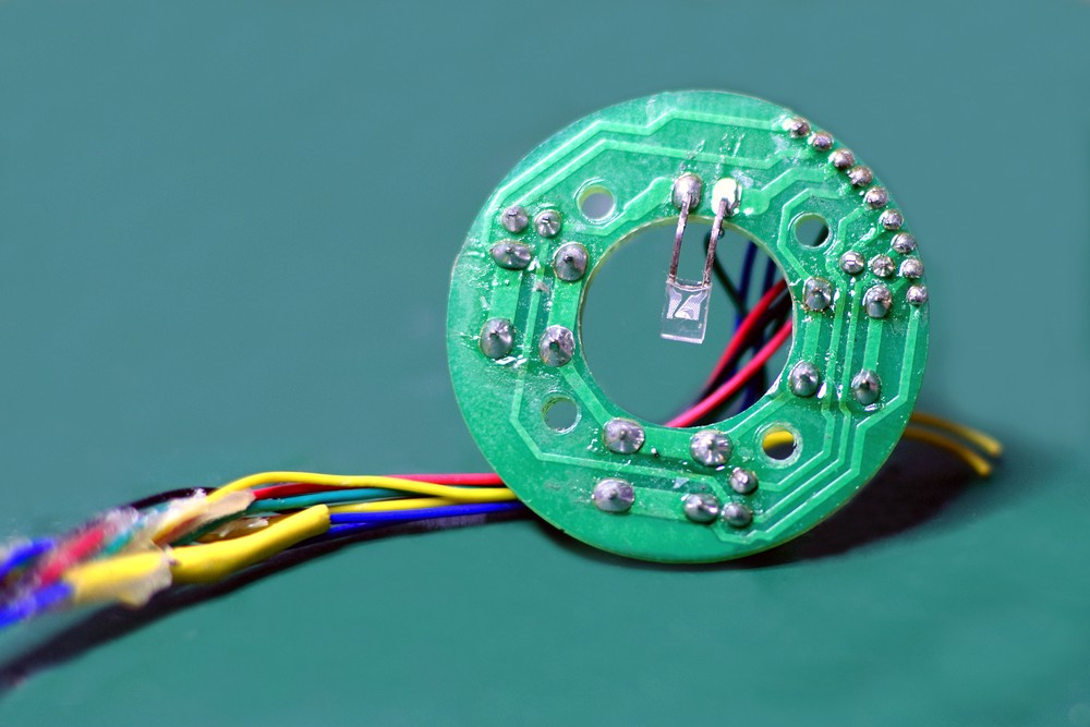
One interesting clothing trend right now is everything getting smaller. Shirts tighter, shorts and skirts shorter. PCBs seem to be following this trend as connected devices get smaller and smaller. Yesterday you had to fit a microcomputer in a watch, tomorrow will it be going inside a thumbtack? You have the skills for a watch, but a thumbtack is another story. As PCB sizes decrease, you will need to be up to date on design shrinking solutions such as efficient fanouts and blind/buried vias.
Integrated circuit (IC) manufacturers are answering the call for small with finer pitch packages, which makes your life more complicated. Things like ball grid arrays (BGAs) and quad flat packages (QFPs) are shrinking, which may require more efficient fanout strategies.
High density interconnect (HDI) boards attempt to save real estate simply by jamming everything as close together as possible. In order to really cram everything in there, you’ll probably need to use buried and blind vias to make efficient connections inside the board.
Beware the dangerous side of smaller, thermal management. A design that worked before may not work if you shrink its layout. Remember to check if your designs can meet heat dissipation requirements with a smaller footprint.
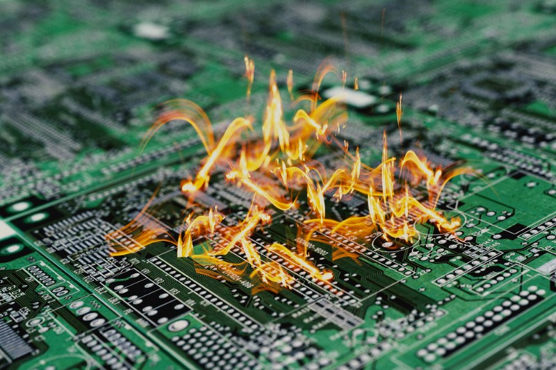
When going fast and small, don’t forget the heat
Faster
Design trends are often at odds with each other, just like you and those teenagers who won’t keep off your grass. The demand for faster circuits has led to designers using more powerful ICs on their boards. Well, usually higher power ICs are larger and run hotter.
With current silicon transistors nearing their minimum size limit we could be looking at a future where chips have to get larger to become faster. As chips get larger, mastery of the efficient design techniques mentioned in the previous section will become more important.
As you well know, more speed means more heat. Hotter ICs will mean planning layouts for thermal management, choosing the perfect thermal interface material, and keeping abreast of new heat dissipation technologies.
Green PCBs
Ever wonder what happens to all those event t-shirts that you wear once and then give away? They eventually get shipped to Africa and find a second life in the dirt cheap used clothing markets. Unfortunately, when PCBs are dumped overseas they are not usually reused.
While many PCBs are green in color, they’re not very green from an environmental standpoint. With a projected 34 billion connected devices by 2020, PCBs will soon need to be a bit more green. PCB designers will soon need to be prepared to make “green” design choices along with the more traditional ones.
Research is now being conducted into using bio-based materials for PCB substrates. There are a wide variety of materials available that could be used in “green” substrates, all with differing mechanical properties.
The advantage is that choosing one or the other will give your board specific mechanical properties, flex, strength, etc. The disadvantage is that designers may soon require the knowledge to choose between chicken feather fibers and keratin fibers for their substrates.
Biobased technologies will also allow substrates to have different electrical properties. The new resins being tested will allow a designer to specify such properties as the dielectric constant for their substrate. I don’t know which dielectric constant to use for specific applications, do you? Designers will soon need to know a lot more about material sciences in order to take full advantage of “green” substrates.

This could be the next IoT application
Training
Keeping up with the latest news and blogs about cutting edge design techniques will definitely help you keep your PCBs in fashion. However, your extracurricular reading should still be supplemented with structured training.
There has been much talk recently about whether or not there is a shortage of PCB design engineers. Whichever side you find yourself on, I think we can all agree that the need for more complex PCBs has left the industry with a shortage of skills. Even when employers find engineers to hire, they often lack the skills required for advanced PCB design.
Those same skills are difficult to obtain. Right now most designers are left on their own to figure out PCB design for themselves. While this method currently works, PCB requirements will soon become so advanced they’ll leave self-taught designers in the dust. Training designers is the only way to ensure that they will have the skills to meet the growing demand for increasingly complex PCB designs.
The world of PCB design is accelerating quickly, and those who do not adapt will be left behind. If you’re worried you might be in that category, talk to your manager about getting some training in new design techniques that can help you design for the future.
A good PCB manufacture can let you make your design dreams a reality. Whether you’re a first-time designer with big ideas for the next great gadget, or an experienced engineer looking to refine your workflow, Juvtmall is better choice for you.
#Juvtmall #PCB #PCBA #hardware
