 USD
USD EUR
EUR GBP
GBP CAD
CAD AUD
AUD JPY
JPY
PCB Design Software and Electronics Design News for PCB designers,
electronics engineers and makers of all kind, visit resources.altium.com and altium.com
Feb 1
High Voltage PCB Design: Creepage and Clearance Distance
When I was an undergrad, I did a lot of electrochemical etching. I put it on my resume for years, because interviewers were always interested in hearing about working with high voltage sources and terrifying chemicals. Later, I realized I didn’t want to be hired for jobs where they wanted someone with a pathological indifference to high-risk work environments.
That was when I started looking into high voltage design. I was amazed by the standards that are required for high voltage products. I was also relieved. While I can’t prevent grad students from McGyvering our high voltage products, I do have peace of mind knowing that there is board level protection in place.
When does safety require specific spacing rules?
Not every PCB design has the same rigorous rules on spacing that a high-voltage PCB design needs. In general, if the normal operating voltage of your product meets or exceeds 30 VAC or 60 VDC, then you should be very diligent about spacing rules in your board design. If you have a high-density board, especially with high voltages, you need to be even more concerned. The high density makes spacing much trickier, and even more important for protection.
Spacing is more important in high voltage designs because the voltage across your board makes it much easier for an arc to occur between two conductive elements on your PCB. Any arc that does occur poses a significantly higher risk to both the product and your users. To help mitigate that risk, there are standards for two primary spacing measurements in your PCB design, clearance, and creepage.
What is clearance?
Clearance is the shortest distance through air between two conductors. I remember its definition by thinking of overhead clearance; how much room in the air before my head whacks into something. If the clearance anywhere on a PCB is too small, then an over-voltage event can cause an arc between neighboring conductive elements on the board.
The rules for clearance vary with the PCB material, voltage, and environmental conditions. The environmental effects are pretty significant. Most commonly, humidity changes the breakdown voltage of air and affects the likelihood of arcing. Dust is another factor since particulates that collect on the surface of the PCB can form a track over time, shortening the distance between conductors.
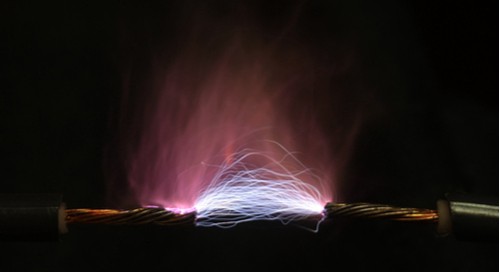
Arcing can damage your product and your users, so spacing on your board is a critical design parameter.
What is creepage on a PCB?
Similar to clearance, creepage measures distance between conductors on a PCB. However, instead of measuring distance in air, it measures the shortest distance along the surface of the insulation material. Board material and environment also affect creepage requirements. Moisture or particulate accumulation on the board can shorten creepage distance the same way they do for clearance.
When you have a high density design, creepage can be a difficult requirement to meet. Since moving tracks is rarely the first choice, there are a couple other tricks for increasing the surface distance in your design. By adding either a slot between tracks, or a vertical barrier of insulation, you can significantly increase the creepage distance without changing the trace layout on the board.
Consider comparative tracking index (CTI) of your material
After operating voltage, the most significant factor in the clearance and creepage requirements comes from the material properties of your PCB. The electrical insulation of the material is indicated by a “Comparative Tracking Index” or CTI value. The CTI is expressed as a voltage and is determined by a standardized test measuring when the surface of the material breaks down.
There are six categories from 0 to 5 based on the breakdown value of the material. The mandatory insulation levels for products are based on these CTI categories. Category 5 is the lowest, with values less than 100 V. With breakdowns of 600+ V, Category 0 has the most robust, and often expensive, material options.
PCB insulator materials have different breakdown voltages and corresponding safety categories for product applications.
How do I know what material and spacing to use?
Because there are so many variables in PCB design and material selection, your best bet for meeting the safety requirements and standards is to go directly to the source. There are two standards I see referenced most often. The first is IPC-2221, which is the generic standard for guidance on PCB design clearance and creepage. The second is IEC-60950–1 (2nd edition). The IEC version is the standard you want to read for any IT products with AC main or battery power, especially if you want to sell those products internationally.
Since the consequences of incorrect spacing vary from legal non-compliance to serious death and destruction, it’s well worth the time to become acquainted with any standards that are relevant to your design. Plus, it keeps the undergrads from zapping themselves.
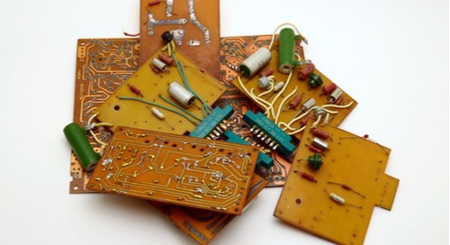
Identifying and incorporating the standards can be time-consuming, so you should use a good design software. The best software for PCB design lets you create specific design rules and helps you identify issues early in the process. Altium Designer fits these requirements and more; you can get started designing even before you’ve chosen your board material!
A good PCB manufacture can let you make your design dreams a reality. Whether you’re a first-time designer with big ideas for the next great gadget, or an experienced engineer looking to refine your workflow, Juvtmall is better choice for you.
#Juvtmall #PCB #PCBA #hardware
