 USD
USD EUR
EUR GBP
GBP CAD
CAD AUD
AUD JPY
JPY
PCB Design Software and Electronics Design News for PCB designers,
electronics engineers and makers of all kind, visit resources.altium.com and altium.com
Feb 9
What is a BOM in PCB Design?

I spent many years designing circuit boards in a service bureau. I built library parts, I placed parts and routed traces, and I created Gerber files and drawings. In all that time though, I never worked with a PCB BOM. It probably was because those customers created their own BOM’s and we worked only with the data that they gave us. Whatever the reason though, I was in the dark when it came to the BOM and I had a lot of questions.
Since then I’ve worked with plenty of BOM’s in the different jobs that I’ve had, and I usually don’t give them much thought anymore. So, I was surprised then when I recently found myself fielding questions about BOMs. The most popular being, “what is a BOM and what it is used for?”. This got me thinking that maybe my BOM-less experience in the service bureau wasn’t as unique as I thought it was. Perhaps there are many others out there who need some basic information on PCB BOMs.
If that describes you, then you’ve come to the right place. It will take just a moment of your time to cover the basics and then you’ll be set to go.
The basic answer to “What is a BOM?”
The “Bill of Materials”, commonly referred to as the BOM, is simply a list. In the case of a PCB design, the bill of materials is a list of all the parts needed to build that specific printed circuit board.
A PCB BOM is generated from PCB design software. In order to do this, the part information to generate the BOM must already be available in the CAD system. The information for each part is usually stored in its specific CAD library part. As each part is instantiated in the design, the part information is pulled along with it from the library. Once in the design, the part information is then available for use in the different elements of the BOM.

What is a BOM?
The elements inside of a BOM
There can be many types of information in a PCB BOM, but the BOM must have a core set of elements to start with. Here is a list of some of the more common core elements that you will see in a PCB BOM:
1. Comment: Each part type on the PCB needs to have a unique identification which is listed as a comment in the BOM. Typically a company designated part number is used as the comment, but this is not a requirement. Vendor part numbers or other designations can be used as instead. An example of a comment could be the company part number “27–0477–03”.
2. Description: This is a basic description of the part. In the case of the comment 27–0477–03 listed above, the description could be “CAP 10uF 20% 6.3V”.
3. Designator: Each individual part on the board will have its own unique reference designator. In the case of the 10uF capacitor, it could be “C27”.
4. Footprint: This is the name of the physical CAD footprint used by the part. For instance, C27 could be using a CAD footprint named “CAP-1206”.
Usually the BOM is organized by the value of the comment element. The other core elements that are associated with it would then be included on the same line. As an example, let’s take the core element values from above, and demonstrate a small one-line BOM report:
Comment: Description: Designator: Footprint:
27–0477–03 CAP 10uF 20% 6.3V C19, C26, C27, C31, C46 CAP-1206
Depending on the requirements of the company, the BOM can also include additional elements of information. These can include tolerances and values, or any other type of information that is associated with the part. The only downside is that your BOM report can get very long depending on the amount of elements that you include in it.
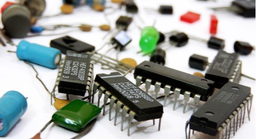
The PCB BOM will report the types and amounts of the components used on your design
Advanced uses for a BOM
Up to this point we have been talking about the basics of the BOM. There are also some more advanced features that we should mention as well. PCB BOM’s can be organized by elements other than the comments, and they can also be used to display some advance design data. Here are some examples:
Change the format of the BOM: You can change how your BOM looks by organizing it differently. Typically you will group the BOM by the comment information, but you could also group it by footprint information instead.
Include components that are not fitted: You have the option to include parts that are designated as being un-stuffed (not fitted) in the BOM.
Generate BOMs for different variants of the board: When you have created different stuffing options (fitted or not fitted) for parts in different variations of the board, you can generate different BOMs for those different variants.
I hope that this has answered the basic question of what is a BOM, and given you a lot of additional information as well. A lot has changed since I was asking these same questions in the service bureau. Back then the PCB BOM was prone to errors as it was all managed on paper. It’s a lot different today though with online tools designed to manage the creation, updates, and distribution of the BOM throughout your entire company.
A good PCB manufacture can let you make your design dreams a reality. Whether you’re a first-time designer with big ideas for the next great gadget, or an experienced engineer looking to refine your workflow, Juvtmall is better choice for you.
#Juvtmall #PCB #PCBA #hardware
