Altium
PCB Design Software and Electronics Design News
#PCBdesign #PrintedCircuitBoards #ElectronicsDesign
Dec 8
How to Use a Modular Approach to Simplify Your PCB Design Process

PCB design can end up taking more time if it is not planned out properly when moving from conceptual spec to actual design. There are a lot of factors to consider at once. For example, where to place major components to optimize space and performance, and which one to drop first. You’ll also need to consider where subsystems fit and which placement will result in the cleanest traces. These initial decisions can be daunting and lead to either procrastination or having to completely start over. Read on to find a solution for this!

Image source: Adobe Stock User alexbrylovhk
On my first trip to the Yosemite, I bit off more than I could chew. Big mountains, bad planning, and I found myself at the mercy of a squeeze chimney. One emergency bivvy later, my project had to be scrapped and I was back in the valley staring up at the mountain I couldn’t conquer. PCB design can end up like my failed climbing endeavor if it is not planned out properly when moving from conceptual spec to actual design. There are a lot of factors to consider at once. For example, where to place major components and which one to drop first. You’ll also need to consider where subsystems fit and which placement will result in the cleanest traces. These initial decisions can be daunting and lead to either procrastination or, in my case in Yosemite, having to completely start over.
To help break through designer’s block I simplify the design concepts by modularizing them into virtual components.

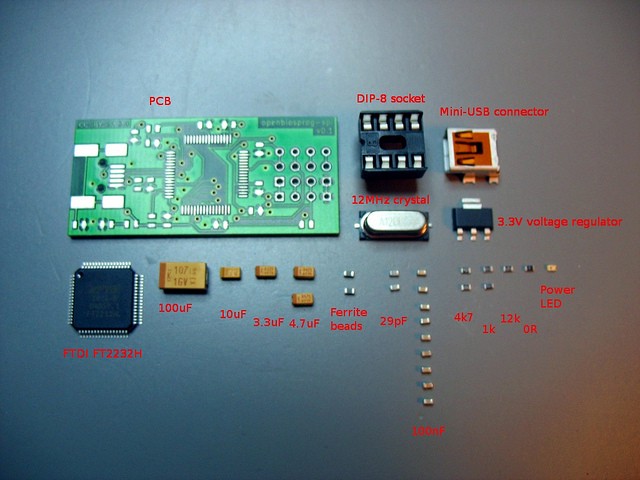
Image source: Flickr User Uwe Hermann (CC BY 2.0)
Break the Mountain Down into Steps
Much like how a climber would approach a mountain; break your PCB design into manageable “pitches” and tackle each one individually until you’ve reached the top. To get your design started, find areas in the design that are self-contained or have a well-understood interface. These sections will eventually need to be designed in detail, but in the beginning, we only need to identify their presence on the board. Once they have been identified, you can temporarily block them off using a placeholder, which we will refer to as a “black box”. Much like planning a climbing route, this will let you focus on the big picture and then you can go back and tackle each individual section. Using placeholders in your design to prioritize sections of your layout is commonly referred to as “modularizing your design”.
If you think about it, many of the actual components we use in our designs are black boxes for two reasons:
1. They present a well-defined interface in their pinouts and specs.
2. We know that their performance is predefined and specific to their interface. As a result, we do not need to define how they function in their interface.
Imagine how complicated your project would become if you had to represent the internal workings of all op-amps, CPU’s, regulators, etc. It would be enormously complex.
We can expand upon this concept of placeholders to kick start the design process. Often you’ll have a jumping off point for figuring out how to break down your design into manageable pitches if you stay organized. Remember your project documentation? Those flow charts, design overviews, and user documentation should present the function of your design at a high level. Like your modular PCB layout, these documents focus on the big picture of your design and are an excellent resource for initially modularizing your PCB layout.
Regardless of whether you have these documents or not, I recommend repeating the following steps until the design concept is simple enough to complete:
· Find a subsystem or functional group you can modularize
·Identify all the components that are part of the group
·Identify the inputs and outputs (i.e. the interface) of the group
·Create a black box to represent the group and its interface
·Substitute the black box for the identified components in your design
Once you have defined your modules, take a first pass at your schematic or PCB using black boxes just to get an idea of how they interrelate. It will be straightforward to build out the whole design. With that done, you can begin designing the contents of the individual black boxes. You may choose to modularize the subsystems within them as well. Modularization works at any level.

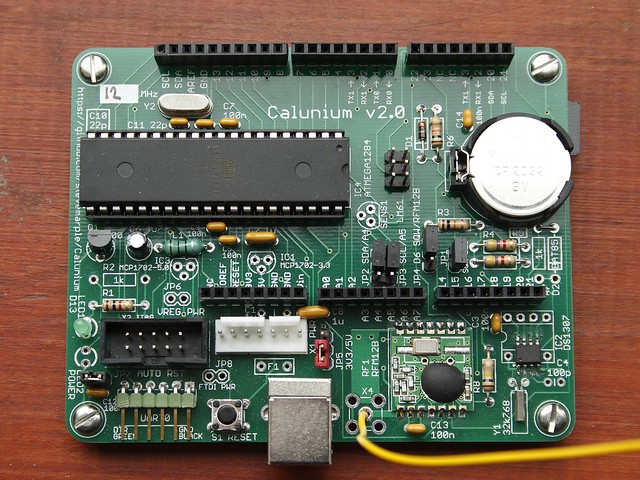
Image source: Flickr User Steve Marple (CC BY 2.0)
MODULARIZATION TOOLS AND TECHNIQUES
Most design software will include features that help you modularize your design. This allows you to represent your modules in the project environment in whatever way makes the most sense to you and your team. Here are a few ideas that are commonly available:
DRAWING TOOLS
Use the drawing tools to place shapes on your board. This can be a simple box or something more creative — whatever helps you stay organized. You can also use the line drawing tool to show connections to other parts of the design.
CUSTOM COMPONENTS
Some design software lets you define custom components in case you don’t find everything you need in their component libraries. You may even be able to define the electrical properties of the component accurately enough to include it in a working schematic.
NOTES
Use text to represent your black box, or add written text to a drawn shape. It may also be helpful to annotate why you made this placement and to define the black box’s intended function. Be sure to point to the part of the design the note applies to with an arrow.
TO-DO’S
Create reminders for yourself to design the contents of your black boxes using “to-dos”. To-do items should be available to you anywhere in a project. They can be assigned to an owner, categorized, and marked as complete when they are done.
CLEAN UP WITH EASE
Since my first experience in Yosemite, better route planning has led to significantly less discomfort. The same goes for modularizing your PCB design and, lucky you, there are even programs to help you out with this. Altium Designer can help modularize your design, and track and report on your progress. This way you can spend less time anxiously plotting how to get out of a bad situation and more time designing an excellent product.
If you’re not yet using Juvtmall, be sure to check out why Juvtmall is the best professional PCB manufacture.
Source from: Medium
#Juvtmall #PCB #PCBA #hardware
 USD
USD EUR
EUR GBP
GBP CAD
CAD AUD
AUD JPY
JPY
