 USD
USD EUR
EUR GBP
GBP CAD
CAD AUD
AUD JPY
JPY
PCB Design Software and Electronics Design News for PCB designers,
electronics engineers and makers of all kind, visit resources.altium.com and altium.com
Jan 30
What Are Molded Interconnect Devices or MIDs?
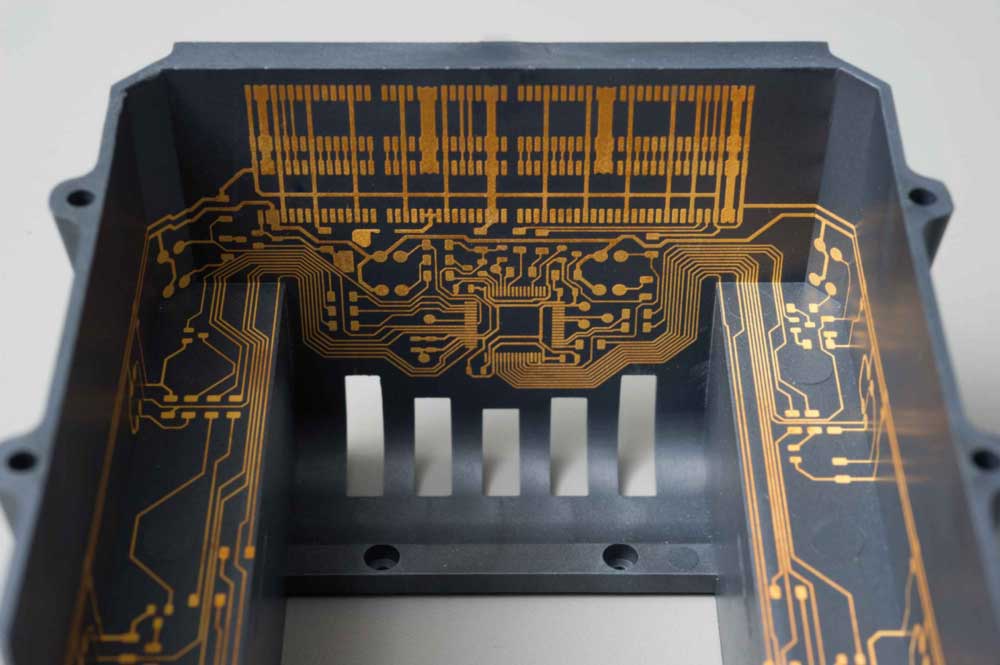
Image courtesy of Fraunhofer IEM
According to MIDIA (Molded Interconnect Devices International Association), a Molded Interconnect Device is an injection molded plastic which incorporates a conductive circuit pattern and integrates both mechanical and electrical functions. It’s the fusion between a plastic part and a circuit. Copper traces are etched onto the surface of the plastic part, creating tracks and pads which can then house electrical components. What you get is a cool electromechanical piece of hardware. That is an MID.
Where MIDs are Used and Advantages of MIDs
You can find MIDs across many industries and products, from medical to automotive industries and also in cell phones and tablets. MIDs make sense for these types of industries and products because of the need to have sleeker designs. Sometimes it’s not practical or possible to have many interconnect components and wires. Phones are a great example of this.
We’re always trying to pack more in a smaller package, so something like a MID can really help us out. By using a molded interconnect device in a phone, we can have the antenna integrated with the mechanical enclosure, saving us space on our board and even giving us a better functioning antenna. These same principles can be applied to any field, including automotive. Below you can see MID technology in a car steering wheel, eliminating the need for wire harnesses.
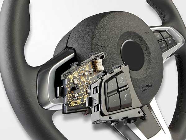
MID technology found in a steering wheel
How Are MIDs Made?
Even though molded interconnect devices have been around for many years, their adoption has not been widespread. MIDs are being used, but so far they will not abolish PCB design as we know it. Because it’s a technology that isn’t widely used, the creation process isn’t as defined, and therefore there are several ways to create a MID.
Two-Shot Molding Process
The two-shot MID process combines two plastics which are molded together to form a single part. The first resin that is shot into the mold is usually not plated because sometimes processes differ between manufacturers. This first injection forms a base for the second shot to build off of; this second shot is highly plateable.
Next, the plastic mold goes through a chemical treatment to promote the adhesion of copper to the mold. After this process, the plastic parts are put through an electroless plating process where copper is deposited on the part as copper traces.
Laser Direct Structuring
Laser direct structuring (LDS) begins with a single shot molding to create the physical part. Then, a laser etches away a thin layer of plastic where the traces will be. Next comes the metalization process where the plastic part is plated with copper.
At this point, you’d have your part go through a 3D pick and place machine where electrical components can be placed.
Metal Spraying
Metal spraying is similar to laser-direct structuring as it uses the same technique up through the LDS process, but it does not make use of a chemical bath to adhere the copper. Instead, as you’ve probably have guessed, it uses a metal spraying technique to deposit the copper on the part. Metal spraying allows for thicker circuitry and also doesn’t need the plastic to be plateable. You may be asking then, how does the metal stick? Well, LDS roughens the surface of the plastic so the metal may easily adhere and stay in place, therefore chemical baths are not needed.
Are MIDs the Future?
Beyond the three processes mentioned above, there are even more processes to create MIDs. This industry is not young, but it is somewhat unexplored, which is why there is no agreed, best method of creating them.
So are MIDs the future? Will they replace PCB design in its current state? I don’t think so, at least not anytime soon. I don’t see MIDs as a replacement to PCBs as they are today, but a means to augment the entire system design.
The reason MIDs didn’t take off in the past is the same reason they aren’t taking off now. The circuit density of these devices is nowhere near as dense when compared to their PCB counterparts. Currently, MIDs can only have two layers, a top and bottom layer, but when you design a PCB, it can have 8, 16, even 32 layers.
Even though MIDs can’t compete with the printed circuit boards of today, that doesn’t mean they don’t have advantages. With MIDs, you’re able to have circuits built into your enclosure saving space, and with miniaturization we certainly need it. What are MIDs? Possibly very helpful in your design process.
Do you have a project to move forward? Find out if Juvtmall is right for you.
A good PCB manufacture can let you make your design dreams a reality. Whether you’re a first-time designer with big ideas for the next great gadget, or an experienced engineer looking to refine your workflow, Juvtmall is better choice for you.
#Juvtmall #PCB #PCBA #hardware
