 USD
USD EUR
EUR GBP
GBP CAD
CAD AUD
AUD JPY
JPY
PCB Design Software and Electronics Design News
#PCBdesign #PrintedCircuitBoards #ElectronicsDesign
Dec 7
How to Design Your Rigid-Flex PCB Within a Board Outline
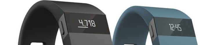
Medical wearables need to be sleek, unencumbered, and compact; able to collect meaningful medical data with few (or no) wires attached to the patient. This creates demand for flexible board designs. While you’re trying hard to push the limits of space, to use smart materials, and to minimize its footprint, it can be damn annoying when you fall out of a board outline (particularly when dealing with irregular board shapes). Read on to find out how to do this!
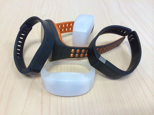
Image source: Flickr User IntelFreePress (CC BY 2.0)
When you were a kid scribbling away in your coloring book your mom probably told you that your pictures were beautiful, despite the fact that you had no regard for coloring in the lines. Well, no matter how much your mom might think that your creations are super special, you really need to keep your PCB design objects within the board outline. This is especially true for those of you who are designing unusually shaped products with rigid flex designs.
As a designer, you know that the demand for flexible PCBs is currently being driven in part by the medical wearables industry. Wearable Internet of Things (IoT) devices are being explored by healthcare professionals for physiological data used for diagnostics, research, and personal health metrics. Moreso, they are changing the way people see fitness by inspiring positive attitudes towards it. Medical wearables need to be sleek, unencumbered, and compact; able to collect meaningful medical data with few (or no) wires attached to the patient. This creates demand for flexible board designs. While you’re trying hard to push the limits of space, to use smart materials, and to minimize its footprint, it can be damn annoying when you fall out of a board outline (particularly when dealing with irregular board shapes).
FUNDAMENTAL BEST PRACTICES TO FOR STAYING AWAY FROM THE EDGE
Before you start making your design specific to rigid flex boards, it’s important that your foundation is correct. You can save yourself a world of pain by keeping these two best practices in check.
Keeping Copper Away From the Edge: Large areas of copper or copper pours (for grounding or carrying power supply for example) are often required on boards. Bringing copper to the board’s edge presents a risk of the layers shorting at the edges when the board is cut. Due to this issue, a best practice has been established for keeping copper at least 15 mil (~ 0.4mm) away from the expected edge. (Protip: Polygon Pours and Copper Regions can be used in Altium Designer.)
Keeping Planes Away From the Edge: Another best practice to keep in mind with your board designs is to pull back planes away from the edge, as this runs the risk of the sides shorting against a chassis.
Basically, the moral of the story is, keep away from the edge from the very beginning so that you don’t have to waste time going back and readjusting your design! That being said, you aren’t totally in the clear unless you consider the types of edges you are working with.
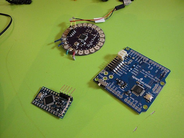
Image source: Flickr User body_pixel (CC BY 2.0)
SUPPORTED EDGE TYPES FOR RIGID FLEX DESIGNS
Working with a rigid flex board means working with specific types of edges. When performing your outline clearance check, it’s important to keep these edges in mind:
· Outline Edge: An important aspect of PCB design and manufacturing is clearly indicating the outline of your board so that your manufacturer will know how to cut the boards. When dealing with rigid flex designs, board geometries may get more complicated than a simple rectangular shape (making clear outlines especially important).
· Cavity Edge: Cavities can create space for placing an integrated circuit within a board substrate. Embedded designs are a favored technique for reducing product footprint, which as we’ve touched upon is an important aspect of designing medical wearables. When dealing with embedded designs, it’s crucial for the designers to be aware of cavity edges.
· Cutout Edge: Sometimes your rigid flex designs may require cutouts. Making sure to clearly define the edges of a cutout is an important design step.
· Split Barrier: The edge defined by a split line. Split lines are increasingly important with multilayer designs. The multilayer approach to circuit board design is advantageous for the medical wearable market in terms of size efficiency.
· Split Continuation: Also known as a permeable boundary. When dealing with multilayer designs you’ll also want to keep this edge in mind. By setting the clearance value for an object-kind to zero, you can instruct Altium Designer that it is allowed to pass over the edge type.
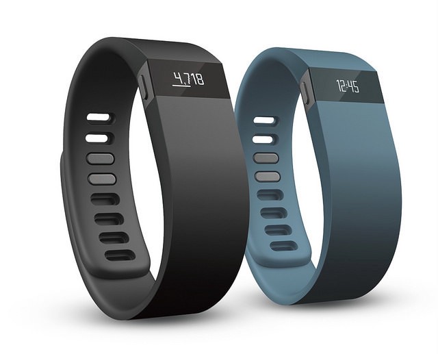
Image source: Flickr User theglobalpanorama (CC BY 2.0)
UTILIZING ALTIUM DESIGNER FOR YOUR RIGID FLEX BOARD OUTLINES
While you’re probably capable of designing within the lines of your board, the right software can make this task easier. The Board Outline Clearance Rule in Altium Designer’s Manufacturing Category has been added in order for designers to specify how close design primitives can be placed to the edge.
By utilizing the Minimum Clearance Matrix in Altium Designer multiple clearances for different pairings can be defined. The alternative is to use a single clearance value for all object-to-edge configurations on your board (but depending on your design this may not always be adequate).
There is a lot more to the edge than just being the lead guitarist in U2. You’ve got to show the edge some respect, and don’t infringe on its territory too much with your designs. Luckily, the correct PCB design layout software will help save you time with planning, so that you can get right into creating.
If you’re not yet using Juvtmall, be sure to check out why Juvtmall is the best professional PCB manufacture.
Source from: Media
#Juvtmall #PCB #PCBA #hardware
