 USD
USD EUR
EUR GBP
GBP CAD
CAD AUD
AUD JPY
JPY
Altium
PCB Design Software and Electronics Design News
#PCBdesign #PrintedCircuitBoards #ElectronicsDesign
Dec 4
How to Maximize Copper in PCB Design: The Pros and Cons of Copper Pouring Versus Placing
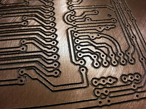
Image Source: Flickr user billautomata (CC BY 2.0)
There is a saying in PCB design, “Copper is free.” It means a PCB designer must think in reverse. A board starts off as solid copper, and the copper you don’t want is removed. It is faster to build, less consumptive, and less expensive to make a board that is mostly copper as compared to the same size board that is mostly bare. Picking the correct technique will make the difference between an effortless or frustrating experience.
The act of maximizing copper is most commonly achieved two ways:
1. Manually — This method is usually faster, but sloppy. By defining and placing specific shapes, copper can be quickly placed as objects. These objects can be assigned to a net and will be checked for shorts or errors during the continuity check. This technique is preferred for quick turns or prototype builds.
2. Automatically — This method is more time consuming; however, a copper pour can better facilitate maximizing copper usage. Instead of laying out the board and then going back and placing copper shapes to fill it in, maximum copper can be left behind by drawing a border around the board area and pouring the copper in.
HOW COPPER POURS CAN SAVE TIME
When pouring copper, a boundary is defined and everything inside it is connected automatically when the pour operation is performed. This technique is usually easier and quicker if the area is large, an unusual shape, or filled with several irregularly shaped objects. A pour operation will automatically fill several irregular areas, additionally, it will automatically isolate other parts or traces in the area.
Objects on the same net, such as ground, will all be connected depending on the setup page or design rules. Objects that a copper pour can automatically handle are vias, traces, nets, decals, voided areas, and pads. Used correctly, copper pouring will automatically make the connections it should and avoid the connections it shouldn’t. These connections can be double checked using the continuity checker tool.
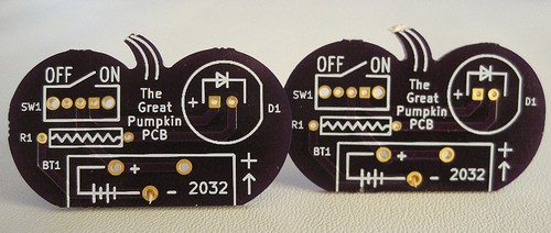
Image Source: Flickr user Low Voltage Labs (CC BY 2.0)
WHEN TO TAKE A MANUAL OR AUTOMATIC APPROACH TO YOUR PCB DESIGNS
A lot of the time we’re inclined to do things manually since it seems like a faster solution in the short term and we don’t need to relinquish control of our designs. However, when you look at the big picture, an automatic approach can be a better long-term option even though it is more work upfront. Here are three situations where using a copper pour might be the better option for your design.
Polygon Management
Manual — If you are making a prototype, don’t waste your time making the design look pretty, especially if the design is guaranteed to change. Creating a conventional closed shape of copper is quick and easy, but when you’re dealing with unusual polygons it can be time-consuming. A quick and dirty technique is to drop overlapping squares, triangles, and trapezoids next to, and on top of, one another to build your shape. While this is useful for short term solutions, eventually you will need to do some vertex editing to clean up your design, which can be tedious.
Automatic — Using a copper pour for this process is automatic in the sense that it stops you from having to manage polygons at all. By defining a border and pouring copper in, you avoid creating objects that will need to be adjusted later if and when changes are made.
Plane Management
Manual — In PCB design a plane is a large area of copper where all connections are one net. If you are building a board with separate planes and adding and changing parts often, it is an easier short term solution to route traces point to point.
Automatic — If your design uses a plane for ground, which is a great way to avoid several traces that all go to the same point, a copper pour is especially effective. Defining and pouring a copper plane will automatically connect all the connections on one net.
Thermal Management
Manual — A quick way to cool down a hot part is to add a big copper square to the decal to help conduct the heat away. This may work best if you have a lot of space to work with, which many times is not the case.
Automatic — You can easily maximize the potential thermal relief by defining an area around your most critical parts, and giving them the priority. Even a matrix of stitching vias can be easily flooded on both sides. Use this when it is important to maximize the copper surface area.
When using copper pours, the time spent defining the rules for connections will allow future designs to be poured perfectly, allowing you to focus on functionality, rather than connectivity. This investment will leverage the time savings into future designs.
Smart Copper Editing can organize these differences in a simple and meaningful way to allow general, marginal, and specific requirements to be automatically applied while pouring copper. Smart Copper Editing can also help manage other areas too, like board edges and unique regions. In design rules, define your vias, traces, nets, decals, voided areas, and pads with specific rules unique to the copper pour.
Having a quality tool like Smart Copper Editing removes the frustration of having irregular copper shapes consume way more time than they should. Save time and avoid the frustration by quickly adjusting your design to meet the requirements you know it must. Contact Altium for more info on their PCB Designer software and how this tool can help you.
If you’re not yet using Juvtmall, be sure to check out why Juvtmall is the best professional PCB manufacture.
Source from: Medium
#Juvtmall #PCB #PCBA #hardware
