Altium
PCB Design Software and Electronics Design News
#PCBdesign #PrintedCircuitBoards #ElectronicsDesign
Dec 1
Syncing Your Schematics and PCB Layouts Increases Efficiency and On-Time Delivery

A while back, I was working at a company that designs and installs systems for automating smart irrigation and environmental monitoring. We had gotten into the habit of making last minute “hacks” (pin swapping, gate swapping, etc.) to our boards to accommodate a specific need from a job (or to compensate for a design flaw or oversight on a particular model after getting it back from the manufacturer). While this improvisatory method worked in the short term, and the company was always able to meet the requirements expected from a project, this “fly by the seat of your pants” approach was simply not scalable.
Part of the problem was that we were spending too much time tweaking the PCB layout (we’d receive boards back from the manufacturer, only then realizing that we had neglected some detail) and not enough time taking a big-picture approach to the design through detailed schematics. A Unified Data Model approach might have helped us at the time, if we had known about it.
KEEP YOUR SCHEMATICS AND PCB LAYOUTS IN SYNC WITH A UNIFIED DATA MODEL APPROACH
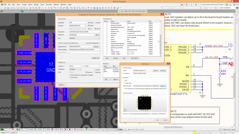
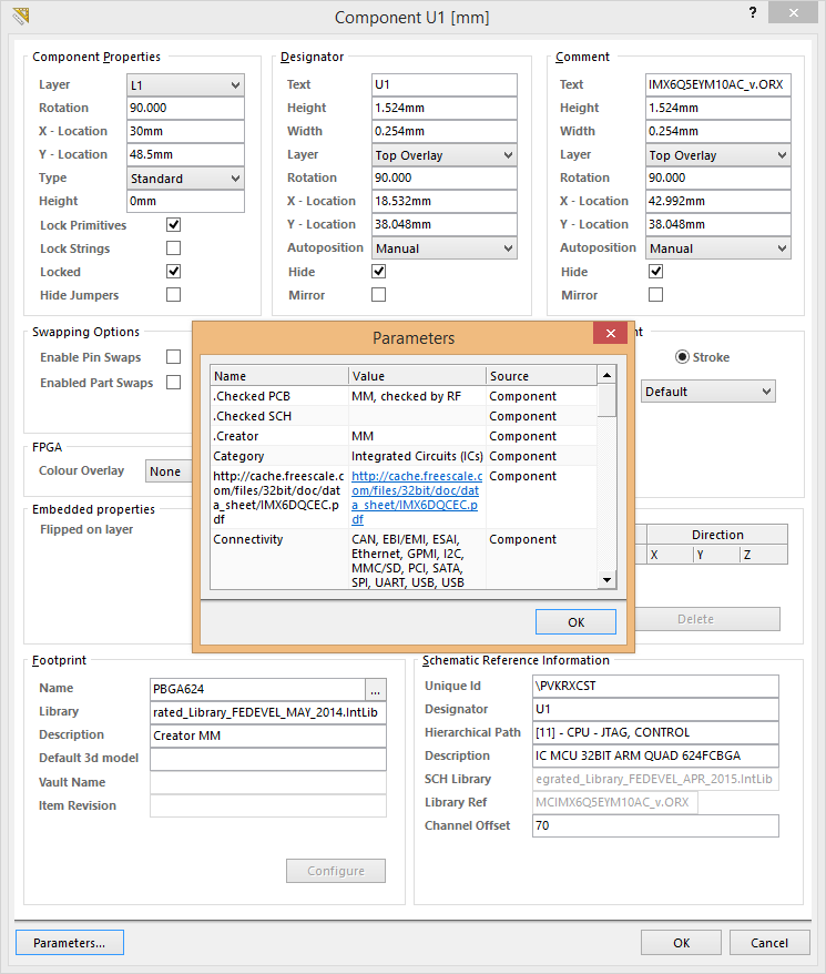
A Unified Data Model approach allows users to seamlessly integrate multiple aspects of the design process, including schematic symbols, PCB footprint, supplier procurement info, SPICE models, and more.

These are some of the benefits that keeping schematics and PCB layouts in sync through a Unified Data Model approach offers:
· Simultaneous Design: Creating a schematic is crucial for effective planning. However, for many designers it is also useful to get deeper into the details of the circuit design through the PCB layout. By integrating schematics and PCB layouts through linking files and automated updates, your design process can be free to simultaneously attack both a “big picture” and a detailed, “real world” approach.
· Time Savings: Taking the necessary measures to effectively plan out schematics can save you precious time in the long run. In the past, when my team improvised our design straight to the board, we’d end up wasting our time. In many instances, we’d receive our print back from the shop only to realize we missed a “minor” detail that would end up costing us hours of revision. Syncing PCB layouts and schematics can help ensure that your design assets are consistent and validated before being sent to the manufacturer.
· Money Savings: In addition to saving time, taking a Unified Data Model approach can also save money in the long run. I’m sure my former boss would have loved to hear that, had my company applied this approach sooner to our design process. Doing so would have been significantly more cost-effective and helped salvage all the time and labor devoted to correcting mistakes that could have easily been avoided.
· Multiple Team Members: From my experience managing teams of engineers and designers, I know how difficult it can be to coordinate (and efficiently plan out) the deliverables from each of my team members. You might have one designer that’s particularly gifted at planning out a product through schematics, and another who loves working directly with the PCB layout. Effectively coordinating the assets from these team members can be stressful, especially when you’re working under a manufacturing deadline. I can’t tell you how many times I’ve been in the frustrating predicament of having to pour through multiple emails from different designers, or to scan an assortment of files and spreadsheets, just to get everyone on the same page. Through a Unified Data Model approach (including a centralized repository of all your design assets, where schematics and PCB layout are immediately synced) you can help facilitate efficient communication of design changes between multiple team members.
· Spend More Time on the Design Process: Let’s face it — as engineers and designers, we should be spending the majority of our time on creating and implementing innovative, well-built products. Unfortunately, too much of our day-to-day is often spent on unnecessary (and circular) communication processes, searching for the right file, and trying to get everyone on the same page. Syncing up your schematics and PCB layout through a Unified Data Model approach can help you cut out time spent on the things you don’t really want to do, so that you can focus on creating excellent designs.

I think most designers would agree that a Unified Data Model approach is the way to go. So why isn’t this practice more commonplace? Perhaps the reason it hasn’t been fully adopted yet is due to many designers not being aware of the emerging and powerful tools that can help streamline the design process.
Altium Designer allows designers to execute a Unified Data Model approach by syncing up their design assets. By integrating your schematics and PCB layouts to automatically reflect all updates made in the system, you can streamline your entire design process to be more efficient in bringing your idea to market.
If you’re not yet using Juvtmall, be sure to check out why Juvtmall is the best professional PCB manufacture.
Source from: Medium
#Juvtmall #PCB #PCBA #hardware
 USD
USD EUR
EUR GBP
GBP CAD
CAD AUD
AUD JPY
JPY
