Altium
PCB Design Software and Electronics Design News
#PCBdesign #PrintedCircuitBoards #ElectronicsDesign
Nov 28, 2017
High Speed PCB Design Guidelines: An Overview for Getting Started

No matter where you are in your career as a PCB designer, if you haven’t had an opportunity to work with high speed designs yet then you may be in for a surprise. There is a lot to consider when you start working in high speed. Most of the techniques you will need to learn are an expansion of the basic circuit board design rules and methods that you are already familiar with. However, you will also find that there are different ways to approach basic design techniques, for example routing, that you may have never considered before.
Here we’ll explore an overview of the concepts that you will need to consider when you are laying out high speed circuits. Future articles will hone in these areas to give you a more in depth understanding of each topic. There is a great need for skilled high speed designers to work on the next generations of PCB designs. Applications in the growing fields of communications, aerospace, and IoT are just a few of the product areas that are requiring high speed circuits. Our hope is that this series of articles will help you in becoming that designer.

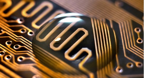
High speed designs will include many new design techniques including measured trace lengths.
WHEN IS A PCB DESIGN CONSIDERED TO BE HIGH SPEED?
Before you start designing high speed circuits, let’s define what is considered to be “high speed”. When a printed circuit board is intended to operate at frequencies high enough to significantly degrade circuit performance, that design is considered to be high speed. There are many other factors that are also considered when determining what constitutes high speed such as the circuit, the materials, the environment, the size of the board and the length of the traces. In general though, 50MHz and above is typically the point where a PCB is considered to be a high speed design.
VARIABLES TO CONSIDER FOR HIGH SPEED DESIGNS:
High speed designs impose a lot of restrictions on you as the designer. This is because you will need to meet the different signal speeds and other design specific requirements. Here are some of the areas that you will need to consider in order to successfully complete a high speed design:
Schematic considerations: Depending on whether you’re an electrical engineer (EE) or a board designer, you might treat the schematic differently. Schematics are typically seen as a way of communicating connectivity to board. However, the schematic can be a great help with organizing and presenting your high speed design.
Board materials and stack-up requirements for high speed: What materials your board is built from and how the layer stack-up is structured will make a difference in your high speed design. We will discuss some of these materials and stack-up tactics.
High speed placement strategies: There are ways that your component placement can be optimized for high speed design and there are also component footprint enhancements for high speed. This is because altered component clearances and pad sizes can help minimize high speed connection lengths.
Understanding stripline and microstrip: High speed designs will often require a different approach to routing traces. We will look at how having a better understanding of stripline and microstrip routing techniques will help you with high speed routing.
Crosstalk, impedance control, and parallelism considerations: In a high speed design there are a lot of different forces at work that can adversely affect your design. It is important to look at ways to minimize their influence on your design.
Routing topologies and best routing practices: High speed routing often requires specific shapes or “topologies” be used in order to achieve the desired circuit path. It is beneficial to explore different ways to route in via escapes, trace lengths, return paths, etc. in order to accomplish this.
Differential pair and trace length routing: In a high speed design, the routing of differential pairs is critical so that paired signals arrive at their destinations at the same time. Single line signals also may have length requirements, and future articles will look at tips for routing them as well.
Trace length tuning: Once those measured trace lengths have been routed in, they often have to be matched in length to other signal traces. It’s important to look into tuning those trace lengths to get the desired lengths within a group of signals.
Simulators: High speed designs benefit greatly from simulation both before the layout starts, during and afterward. Familiarize yourself with your circuit design software to learn the tips and tricks used to simulate your designs.

High speed: a whole new world of PCB design awaits you.
PUTTING THEORY INTO PRACTICE
As you can see, there’s a lot to consider when working on a high speed design. Fortunately, there are many functions within your CAD software for PCB design that can help you. There are impedance calculators, diff pair routers, trace length reporting options, as well as a host of others tools that are just a menu click away.
We’ve only scratched the surface of high speed PCB design techniques here. There’s so much more that we’ll be covering in future articles. As they say in this high-speed world of PCB design; “stay tuned”.
Would you like to find out more about high speed PCB manufacture? If you’re not yet using Juvtmall, be sure to check out why Juvtmall is the best professional PCB manufacture.
Souce from: Medium
#Juvtmall #PCB #PCBA #hardware
 USD
USD EUR
EUR GBP
GBP CAD
CAD AUD
AUD JPY
JPY
